Looking at the picture posted by user “M3NTAL” to SBAF (the same that is in the OP here), I would say that is more than a claim.
I got another 2 pcb photos showing the same chip (probably an Op-Amp) blowing up.
Here is the photo of the back of the PCB by “M3NTAL”. The black spot in the Serial Number spot indicates something got pretty toasty. This is the only photo I have of the back (of a blown up L30).

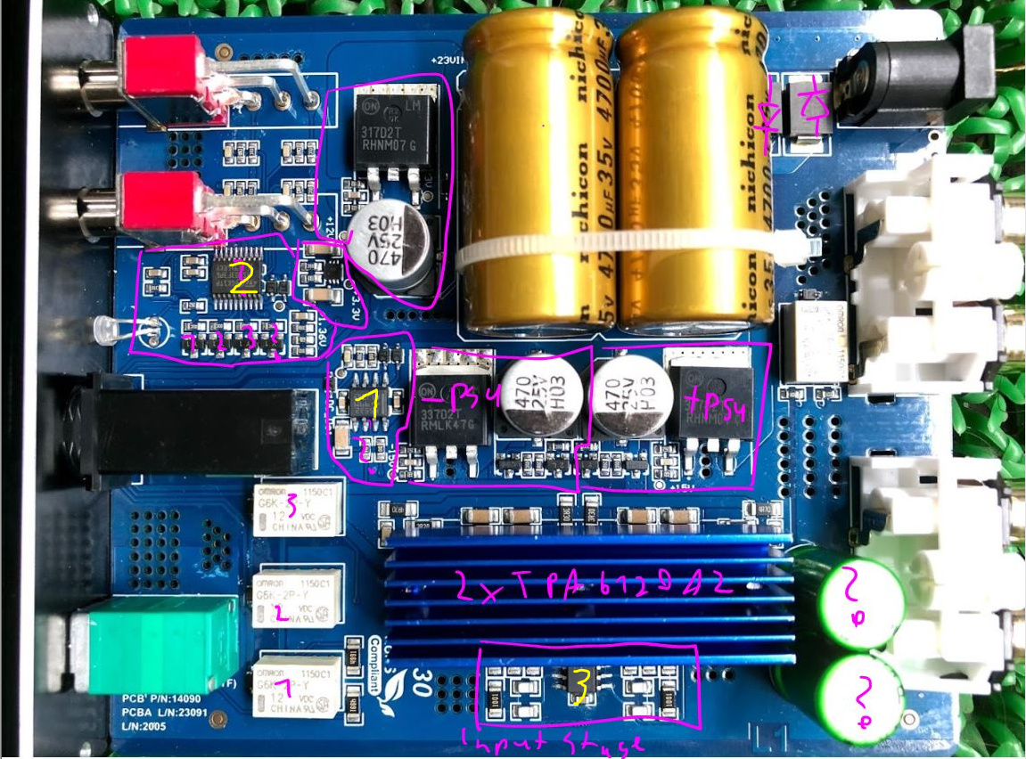
Concerning the layout of the L30: I looked at it a bit now trying to figure out how these can blow up. As I don’t have one myself (or access to my unis electronics labs), I am flying somewhat blind here, so take a grain of salt with the following:
(Picture from ASR review, with my markings)
-
There is no fuse or NTC thermistor to limit fault current in case of a component failure
-
There are no protection mechanisms against overvoltage on the input, like a Varistor
-
There is a circuit marked “DC_Det” (Marked yellow 1 in the picture). Given its proximity to the headphone jack, I assume that is an Op-Amp to detect DC components on the output. Question is if that controls one of the relays (marked pink 1, 2 & 3) or just reports to what I assume is a micro-controller (marked yellow 2). The Transistors below the uController suggest it being in charge of operating the 4 relays in the device.
-
Supply rails are provided by LM317, LM337 and one chip next to the Micro-controller. Except for the unidentified chip between the uController and the top-left LM317, all of these are LDOs. Due to their design, these will current limit to 1.5A continuous (1.5A @ 15V ≈ 22W).
-
There is a pair of Texas Instruments TPA6120A2’s under the blue heatsink. I don’t know how these behave when exposed to DC accross their input terminals.
-
Op-Amp (marked yellow 3) is what fails catastrophically and probably short circuit exposing the two TPA6120A2’s to DC.
-
There are Flyback (= Freewheel) Diodes next to all 4 relays.
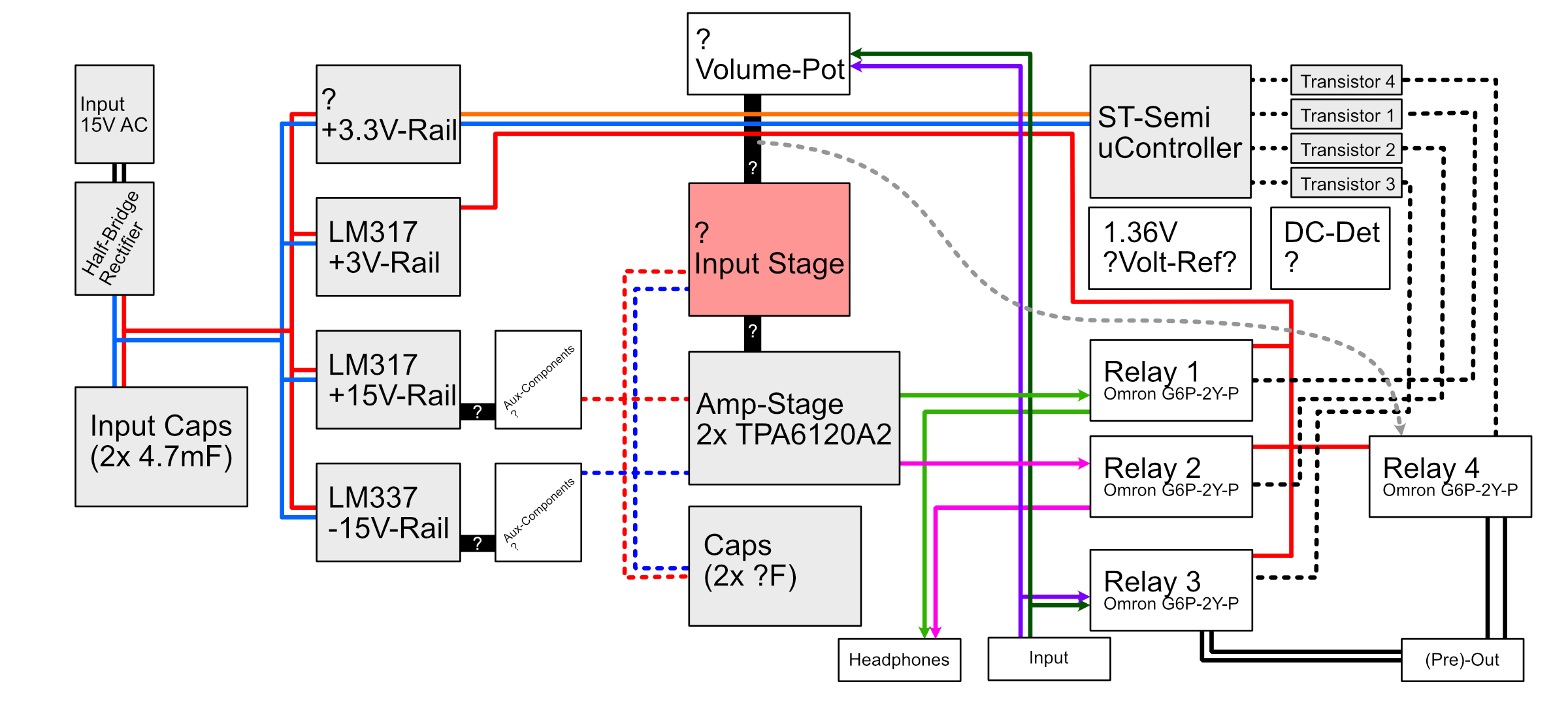
Block Diagram
This is drawn from the pictures I have and the datasheets for components I could identify.
Solid lines and solid arrows are what I am reasonably certain about.
Dotted lines, dotted arrows and ?-marks identify components and connections I am unsure about.
The red box marks the group which failed.
Concerning some of the theories I found on various sites:
-
This is not caused by ESD!
Op-Amps may be damaged by ESD. ESD will not cause burn marks on the back of the PCB though! As the Op-Amp is sanded down , it is anyones guess what make and model it is. So “known failure modes” of the Op-Amps can not easily be determined.
 -
Anything under 22V DC on the input does not cause this. 15V AC rectified comes out to ~21V DC. Running the L30 off USB will not achieve anything as the TPA6120A2’s will not turn on.